I validated RayRF's PMC boundary against a 2003 IEEE paper, with openEMS as referee
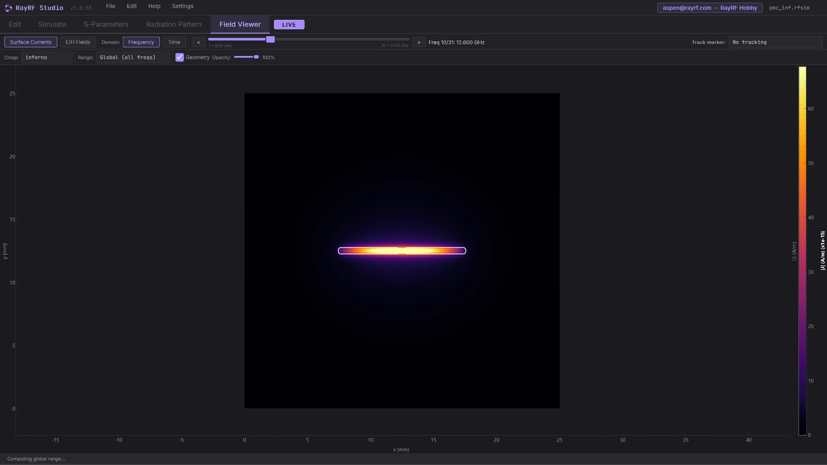
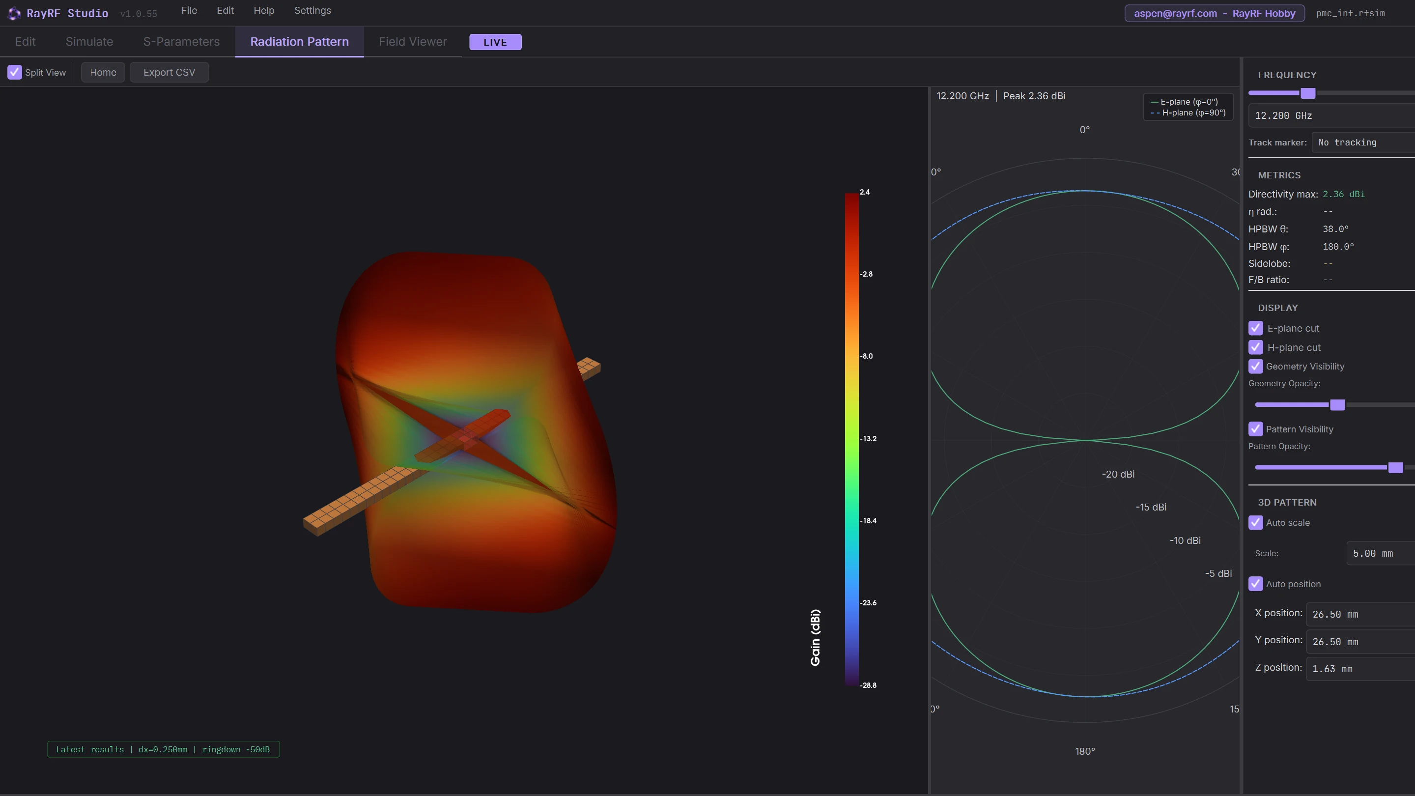
A PMC is the one boundary you cannot check on a bench, because the material does not exist. When I added it to RayRF I wanted more than the internal physics tests passing. So I pulled a paper that RF engineers have cited for two decades, rebuilt its reference cases at the exact published dimensions, and then made a second, independent solver judge the same geometry cell for cell.
The paper
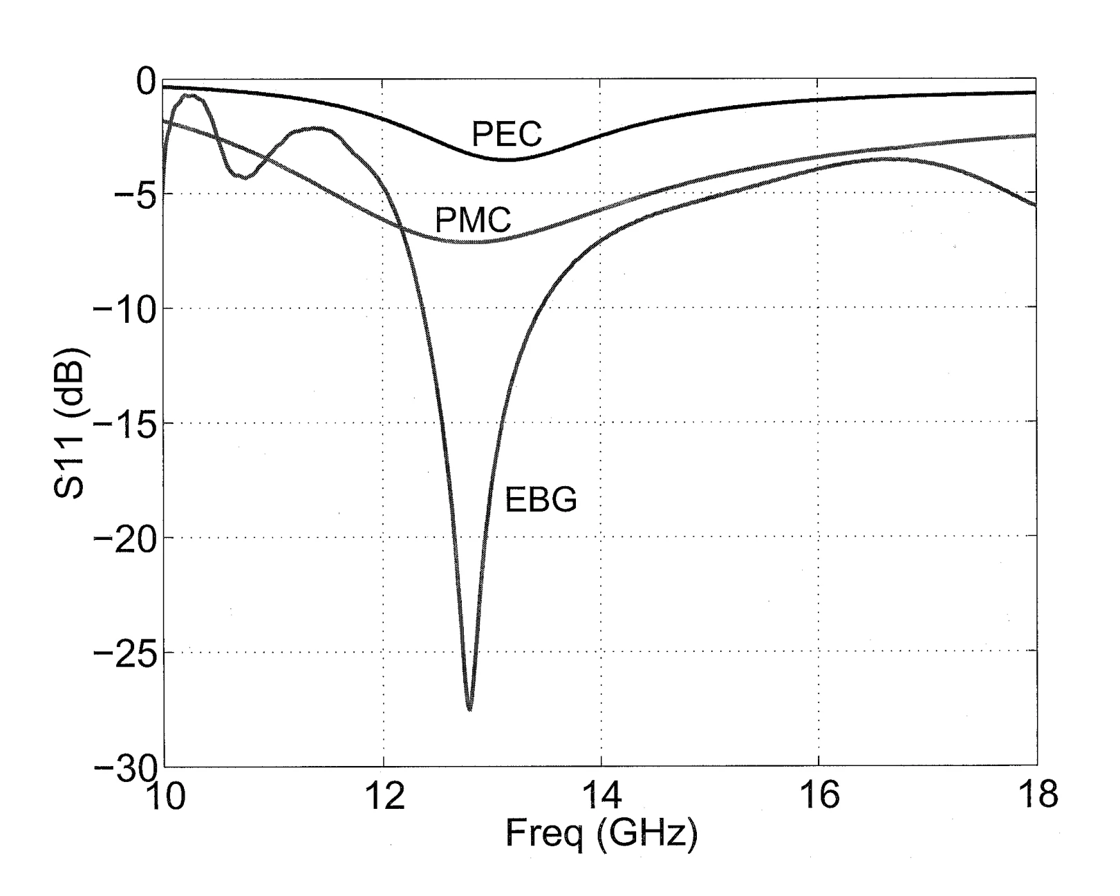
Fan Yang and Yahya Rahmat-Samii, "Reflection phase characterizations of the EBG ground plane for low profile wire antenna applications," IEEE Transactions on Antennas and Propagation, vol. 51, no. 10, pp. 2691-2698, October 2003. It is one of the standard references for electromagnetic band-gap ground planes. Before getting to the EBG surface, the authors set the stage with a clean question: what happens when you put a half-wavelength-class dipole extremely close to an ideal ground plane of each polarity?
Their Figure 3 answers it with FDTD. Over a PEC, the dipole's return loss never gets below -3.5 dB. The anti-phase image current 3 mm away kills the radiation, and the feed sees a near-short. Over a PMC, the in-phase image shifts the input impedance off 50 ohms instead, and the dipole manages a moderate -7.2 dB dip. Their mushroom EBG surface reaches -27 dB. I replicated all three configurations. The one thing I did not replicate is the paper's separate reflection-phase characterization of the infinite EBG surface, which needs periodic unit-cell boundaries and a plane-wave source RayRF does not have.
The setup
Everything is defined relative to the free-space wavelength at 12 GHz, which is 24.98 mm. The dipole is 0.40 wavelengths long with a wire radius of 0.005 wavelengths, centered 0.06 wavelengths above a one-wavelength-square ground plane, fed at the center against a 50 ohm reference. RayRF draws planar copper, so the round wire becomes a flat strip using the standard equivalence of strip width equals four times the wire radius. On the 0.25 mm reference mesh the worst dimension snap is 0.07 percent:
| Quantity | Paper | RayRF | Cells at 0.25 mm |
|---|---|---|---|
| Dipole length (tip to tip) | 9.993 mm | 10.0 mm | 40 |
| Strip width (4x wire radius) | 0.4997 mm | 0.5 mm | 2 |
| Feed gap (center, in-plane port) | not stated | 0.5 mm | 2 |
| Height above ground | 1.499 mm | 1.5 mm | 6 |
| Ground plane side | 24.98 mm | 25.0 mm | 100 |
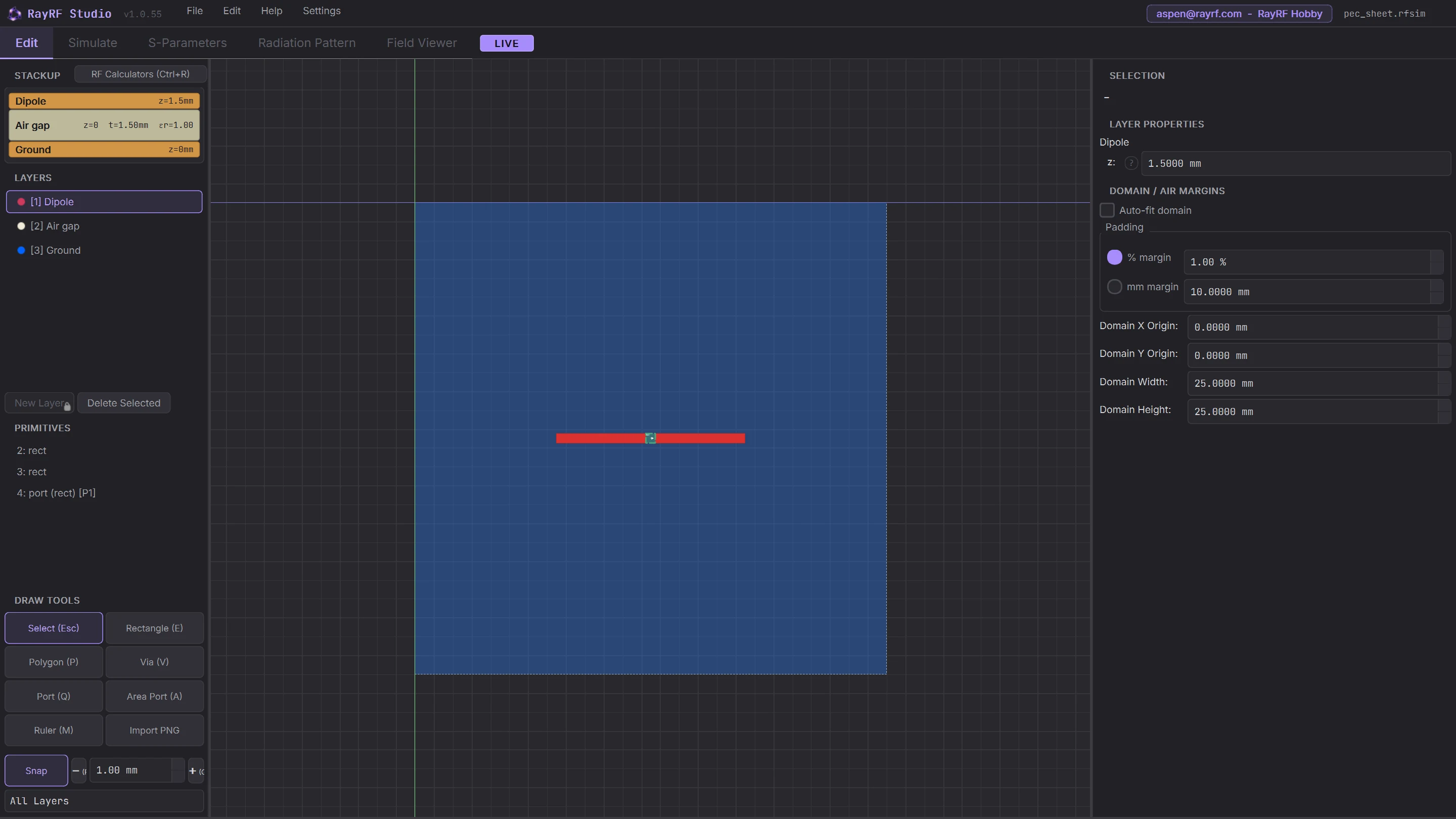
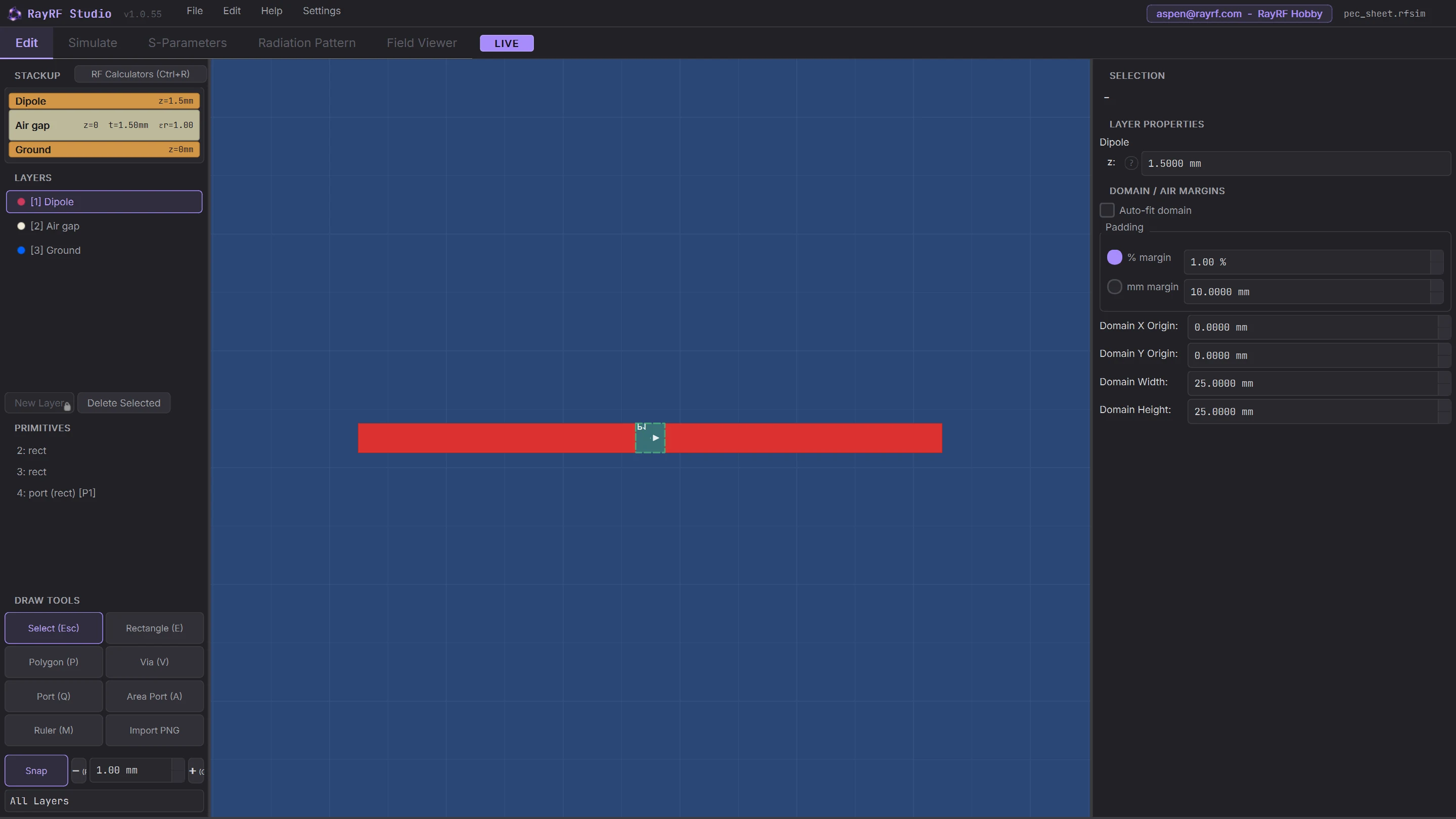
Two RayRF features carry this whole exercise. The first is the in-plane port direction that shipped alongside the boundary work: a printed dipole needs its excitation across a horizontal gap on a single copper layer, not the vertical probe a patch uses. The second is the per-face boundary matrix. For the ideal-ground cases there is no copper sheet at all: the bottom face of the simulation domain itself is the ground plane, set to PEC or PMC with a fixed 1.5 mm spacing below the dipole. That makes the ground mathematically infinite, which is exactly what the textbook image-theory check assumes.
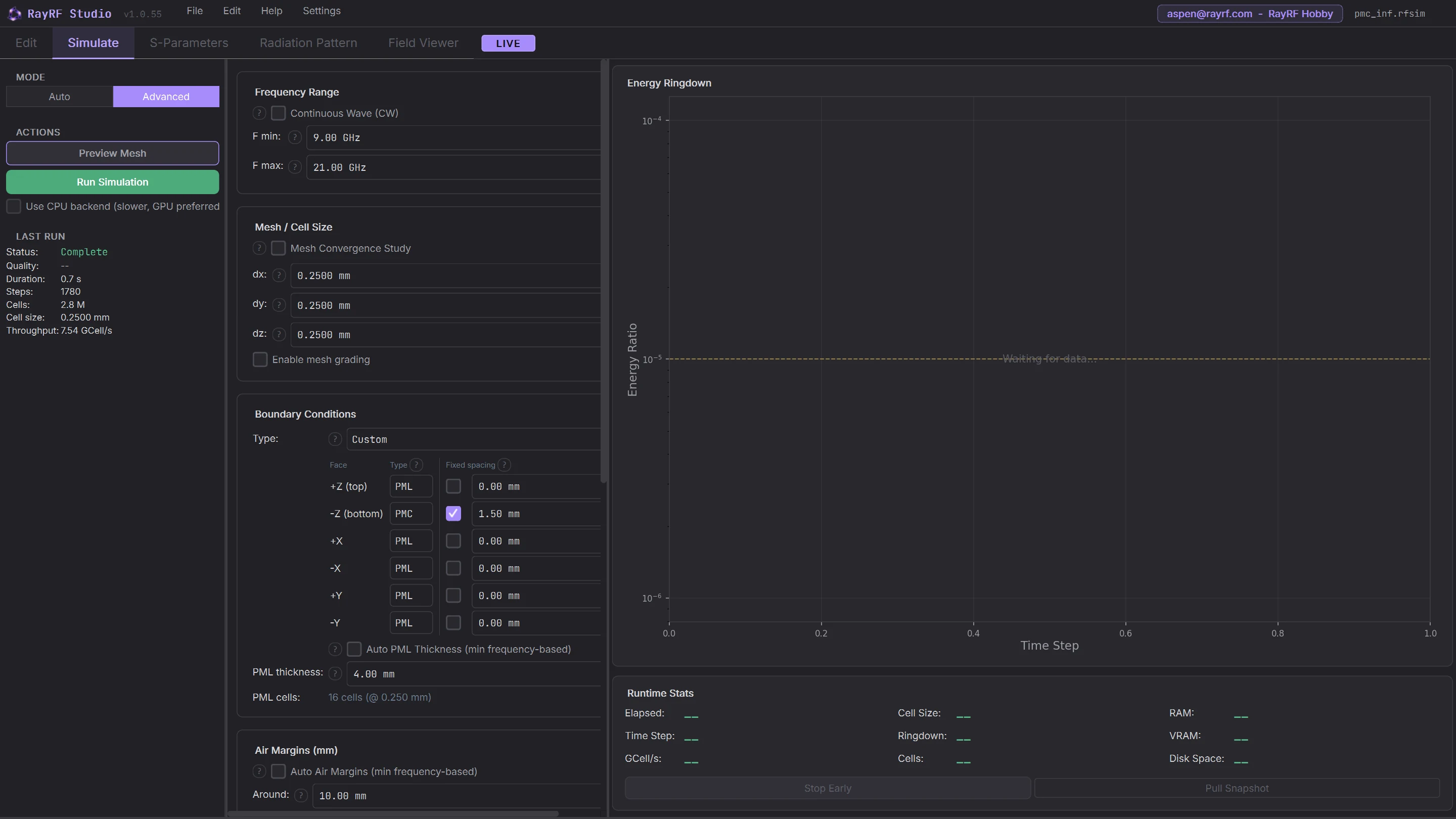
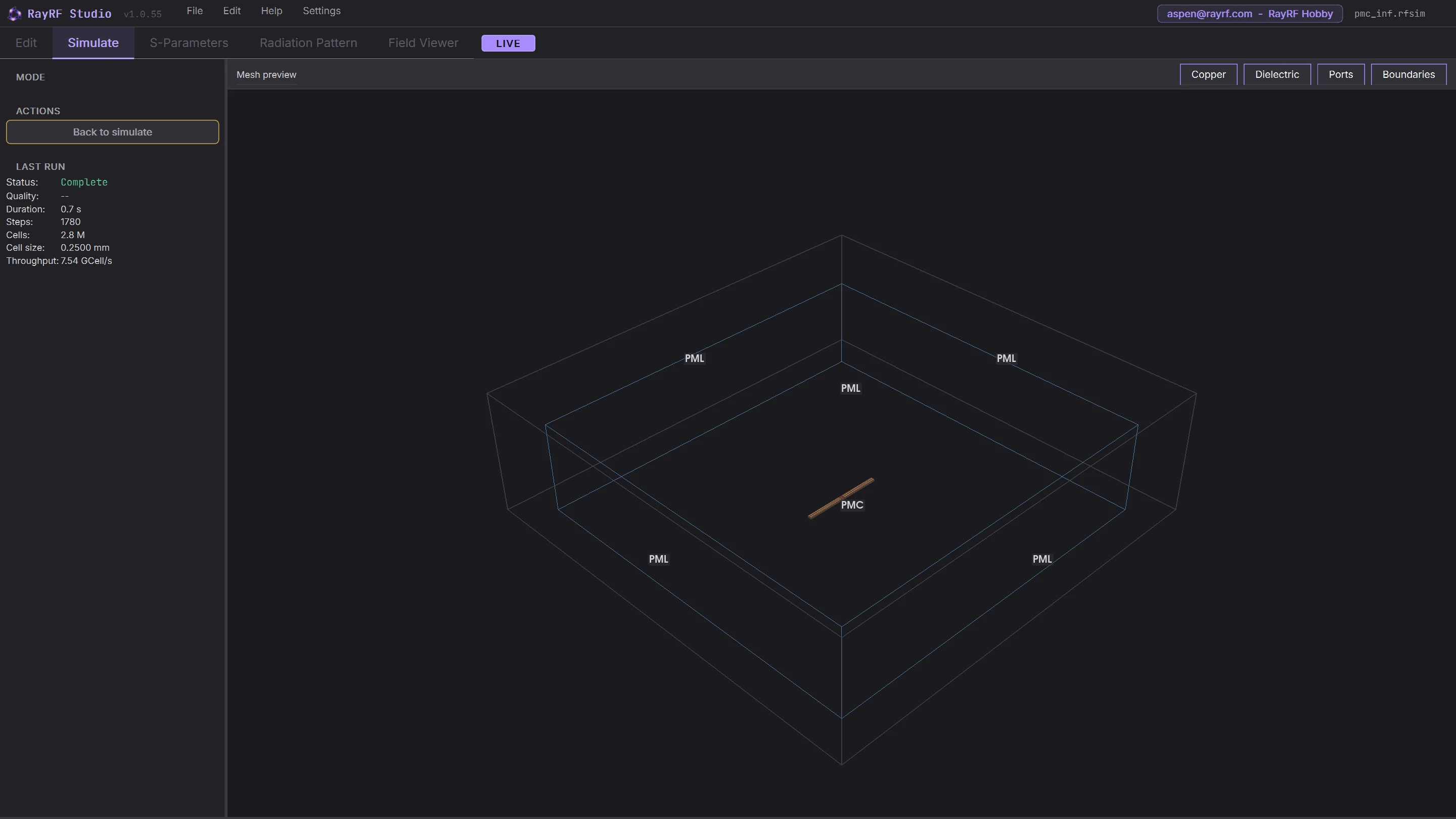
All RayRF runs in this post are the CUDA backend on an RTX 5070 Ti, which runs these domains at 16 to 22 GCell/s. Every run ends on the solver's own energy ringdown criterion, with the step cap raised to one million so nothing terminates early. That matters for the EBG, which rings two orders of magnitude longer than the bare dipole cases.
Results: the dipole over PEC and PMC
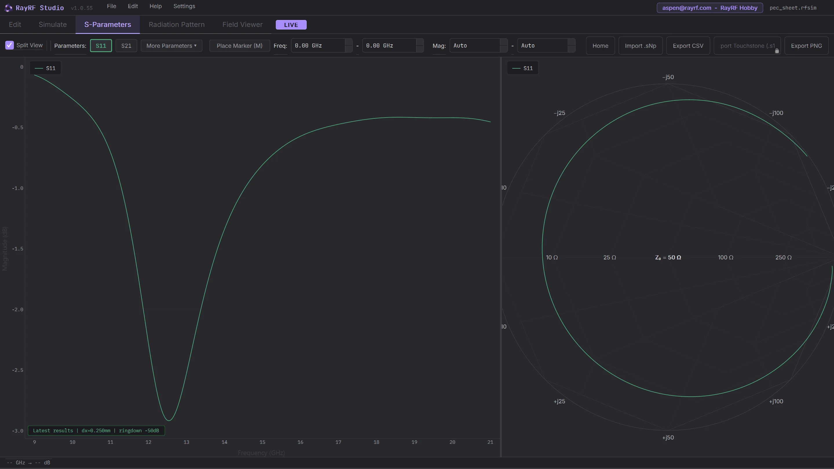
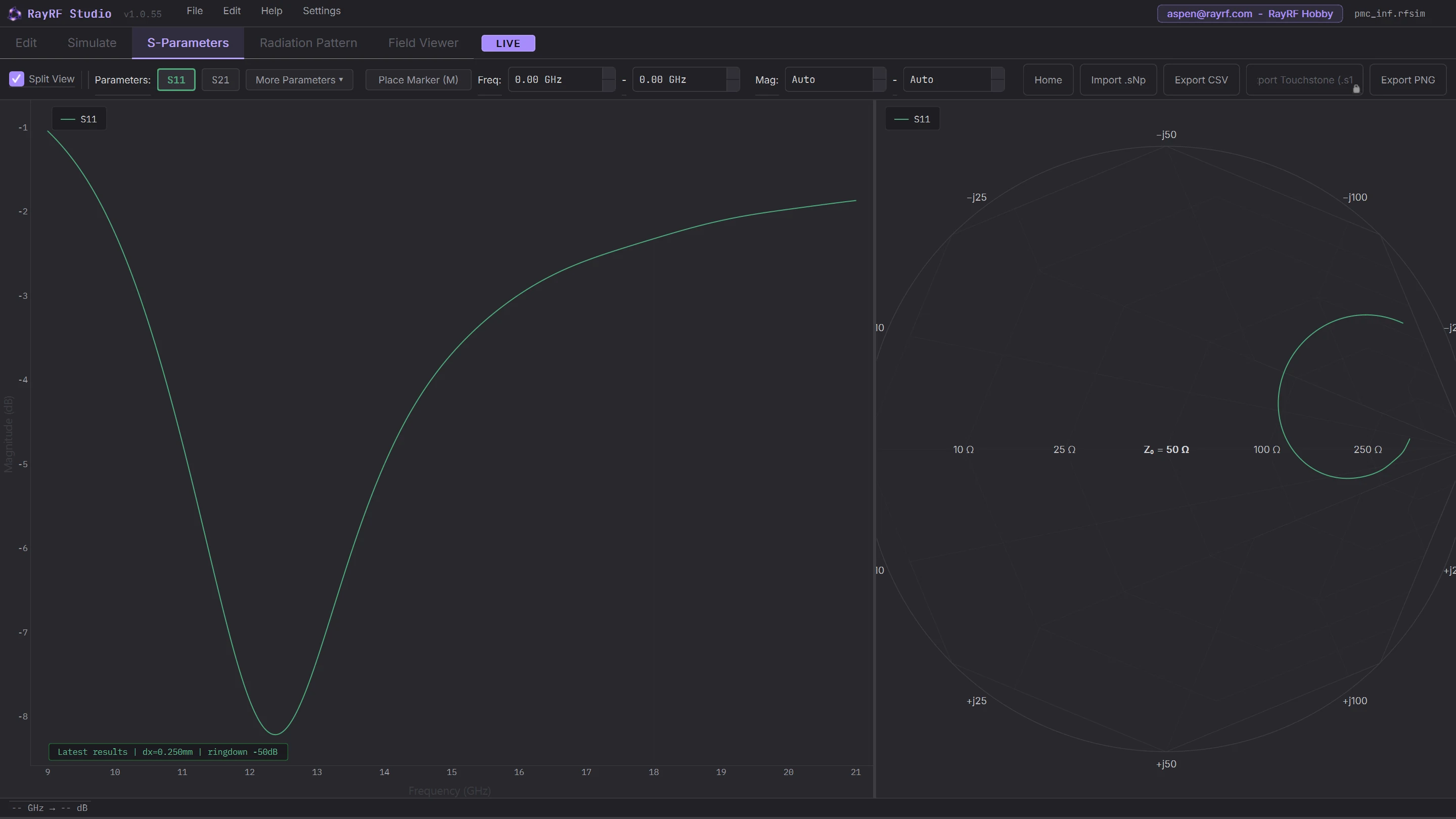
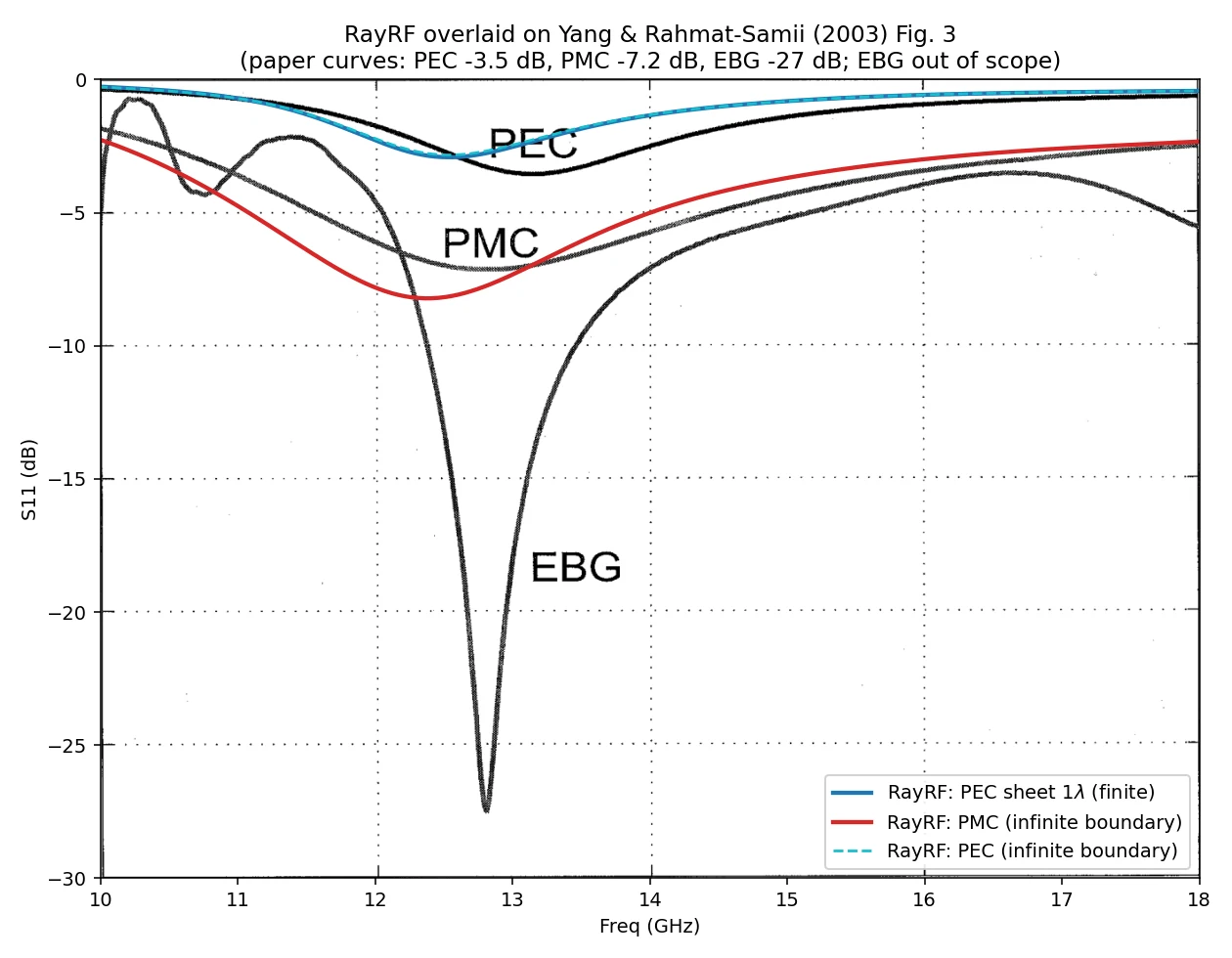
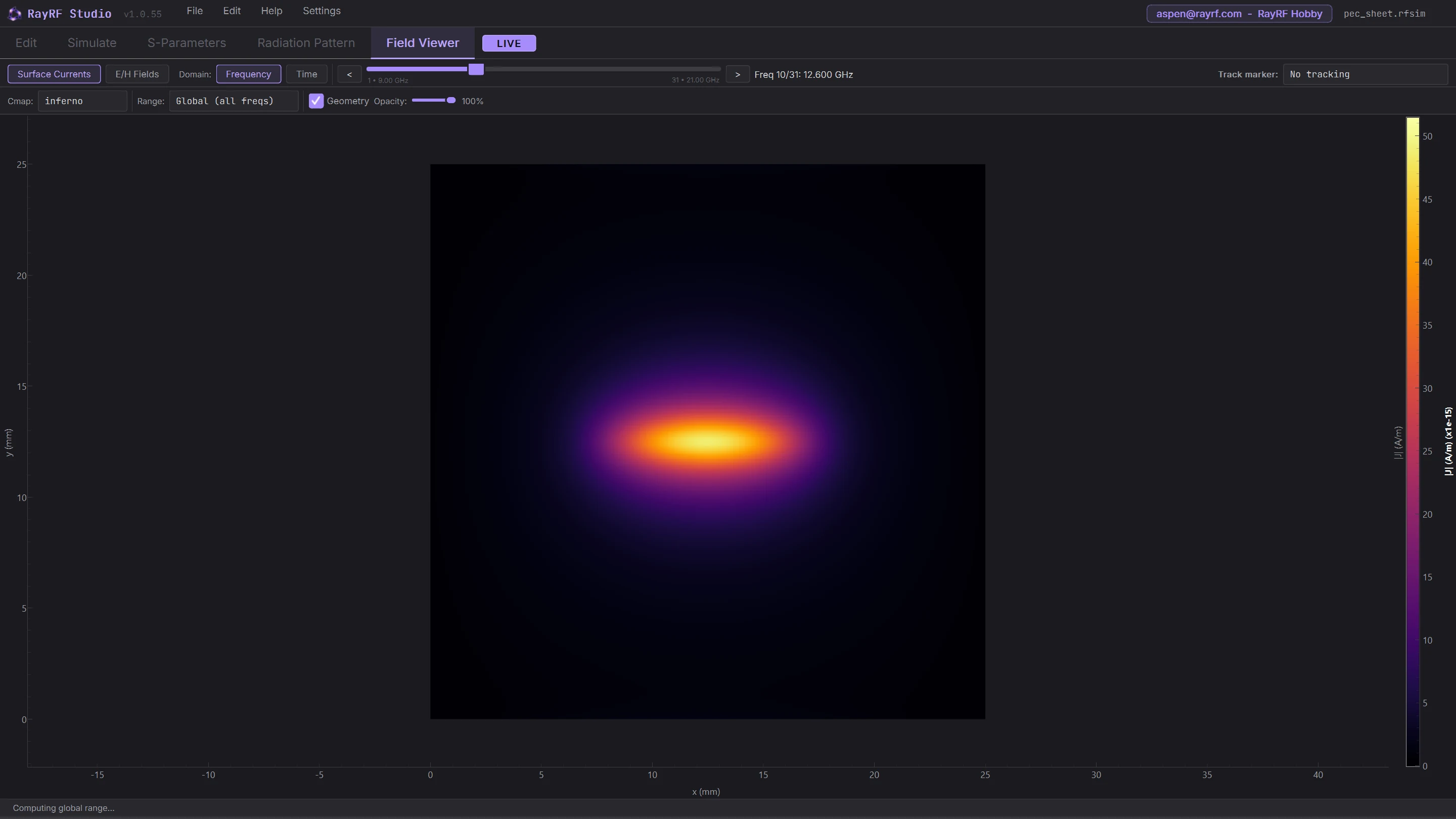
The behavior is the paper's, feature for feature. Over PEC the dipole refuses to match anywhere in the band, bottoming out at -2.9 dB against the paper's -3.5 dB. Over PMC it manages -8.2 dB against the paper's -7.2 dB, with the dip 2.5 percent below where the paper's curve reads. The ground-size checks came out the paper's way too: going from the 25 mm sheet to a 50 mm sheet moved the PEC dip by 0.09 dB, and replacing the sheet with the infinite wall changed nothing past the second decimal. At 1.5 mm height the image current dominates and the plane's edges are spectators.
A second referee: the same cases in openEMS
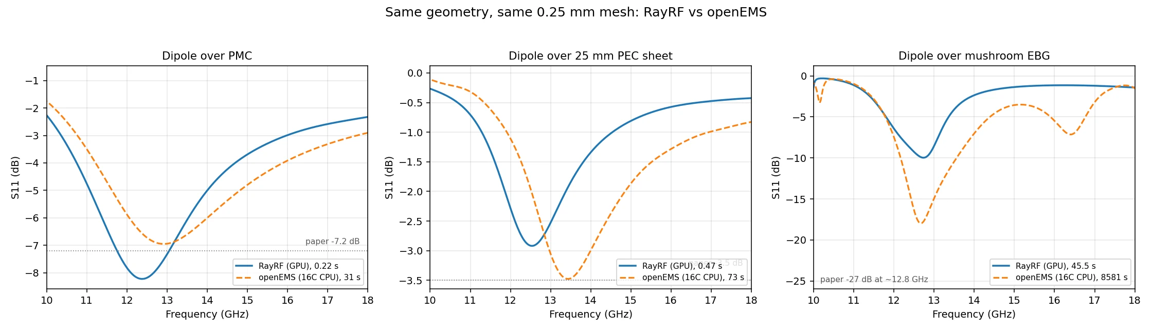
Agreement with a 23-year-old plot read by eye only goes so far, so I rebuilt the same cases in openEMS, the open-source FDTD this machine already runs for benchmarks. Same coordinates, same uniform cell size, same band and port, PML on the same faces, and openEMS's own PMC boundary on the bottom face for the ideal-ground case. Both solvers ran to their own ringdown criteria. That makes openEMS an independent referee on identical input, with only each engine's internal discretization choices left to differ.
| Case | RayRF | openEMS | Difference | Paper |
|---|---|---|---|---|
| Free-space dipole | 12.46 GHz, -19.7 dB | 13.25 GHz, -15.5 dB | 6.1% | not shown |
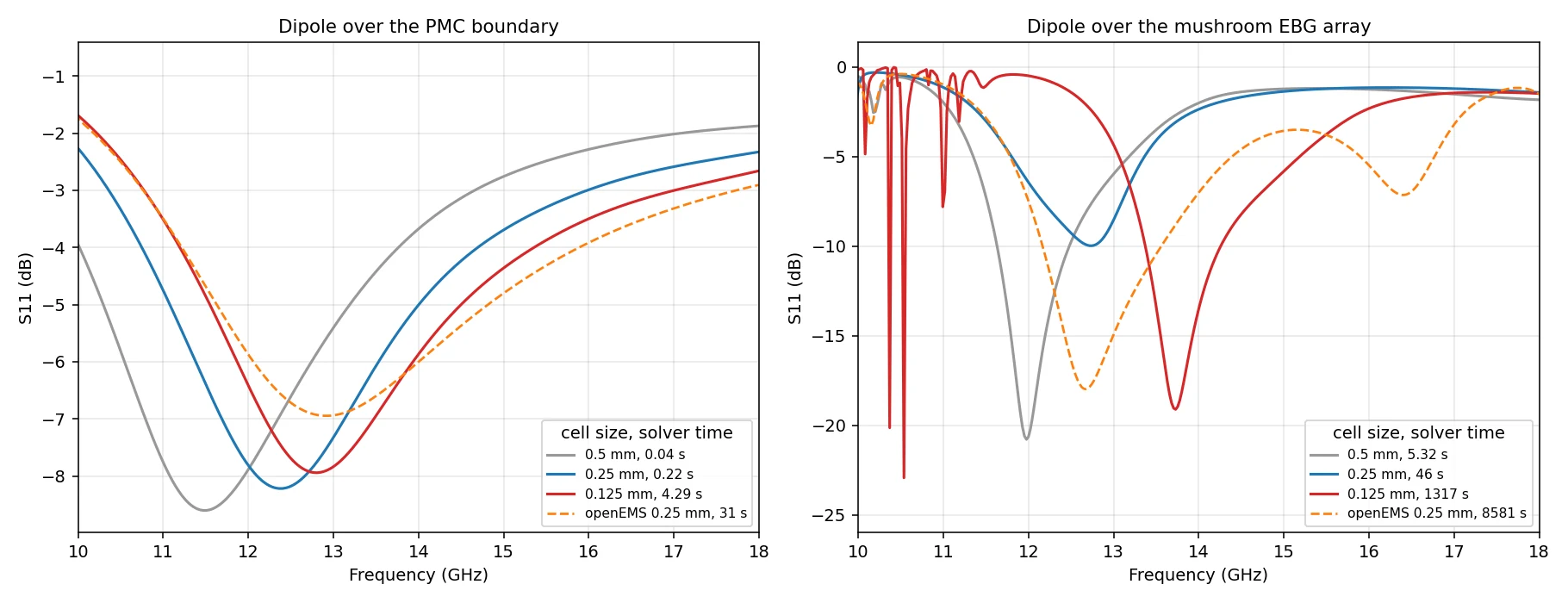
| Dipole over PMC | 12.38 GHz, -8.2 dB | 12.91 GHz, -7.0 dB | 4.2% | -7.2 dB |
| Dipole over PEC sheet | 12.53 GHz, -2.9 dB | 13.44 GHz, -3.5 dB | 7.0% | -3.5 dB |
| Dipole over EBG array | 12.72 GHz, -10.0 dB | 12.67 GHz, -18.0 dB | 0.4% | -27 dB at ~12.8 GHz |
The dipole cases differ by 4 to 7 percent between the two solvers, and the free-space row explains why. The exact same strip on the exact same grid resonates at 12.46 GHz in RayRF and 13.25 GHz in openEMS, against a converged value of 13.46 GHz. The two engines rasterize a 2-cell-wide zero-thickness strip differently, RayRF running it about 7 percent electrically long at this cell size and openEMS about 2 percent. That is a property of staircased thin strips at coarse cells, not of any boundary, and the paper's own in-house FDTD carried the same class of offset. The EBG row is the quantity this paper is actually about, and it lands within 0.4 percent across two independent codes.
What different run times buy you
Validation numbers mean little without the cost attached, so here is the same physics on three uniform meshes, every run ringdown-terminated. The 0.5 mm rung matches the cell size the paper's own 2003 FDTD implies. Solver time is the stepping loop on the RTX 5070 Ti:
| Case | Cell size | Cells | Solver time | Dip | S11 |
|---|---|---|---|---|---|
| Dipole over PMC | 0.5 mm | 0.35 M | 0.04 s | 11.50 GHz | -8.6 dB |
| 0.25 mm | 2.8 M | 0.22 s | 12.38 GHz | -8.2 dB | |
| 0.125 mm | 22 M | 4.3 s | 12.79 GHz | -7.9 dB | |
| Dipole over PEC sheet | 0.5 mm | 0.66 M | 0.05 s | 11.59 GHz | -2.0 dB |
| 0.25 mm | 5.3 M | 0.47 s | 12.53 GHz | -2.9 dB | |
| 0.125 mm | 42 M | 8.4 s | 13.08 GHz | -3.3 dB |
The physics verdict, poor match over PEC and a moderate dip over PMC, is already correct in the 0.04 second run. What refinement buys is the dip position, pinned by the free-space anchor above. For scale, openEMS needs 31 to 73 seconds on 16 cores for the middle rung of these cases. RayRF's GPU engine clears all six ideal-ground runs in under 14 seconds combined.
The independent referee: image theory
For an infinite plane, image theory is exact: the ground is replaced by a mirror dipole at twice the height, anti-phase for PEC, in-phase for PMC, and the input impedance follows from the self and mutual impedance of a two-dipole pair. I computed that with the induced-EMF method, a few dozen lines of numpy that know nothing about FDTD. Two checks fall out of having both ideal-wall runs, and they cancel everything about my modeling choices:
- Superposition: the average of the PEC and PMC input impedances must equal the free-space dipole's impedance, point by point. In the 10 to 14 GHz band that holds within 4 ohms on a 77 ohm scale, about 5 percent.
- The half-difference of the two runs isolates the image contribution itself. Its resistive part matches the analytic mutual impedance within about 3 percent RMS over the same band.
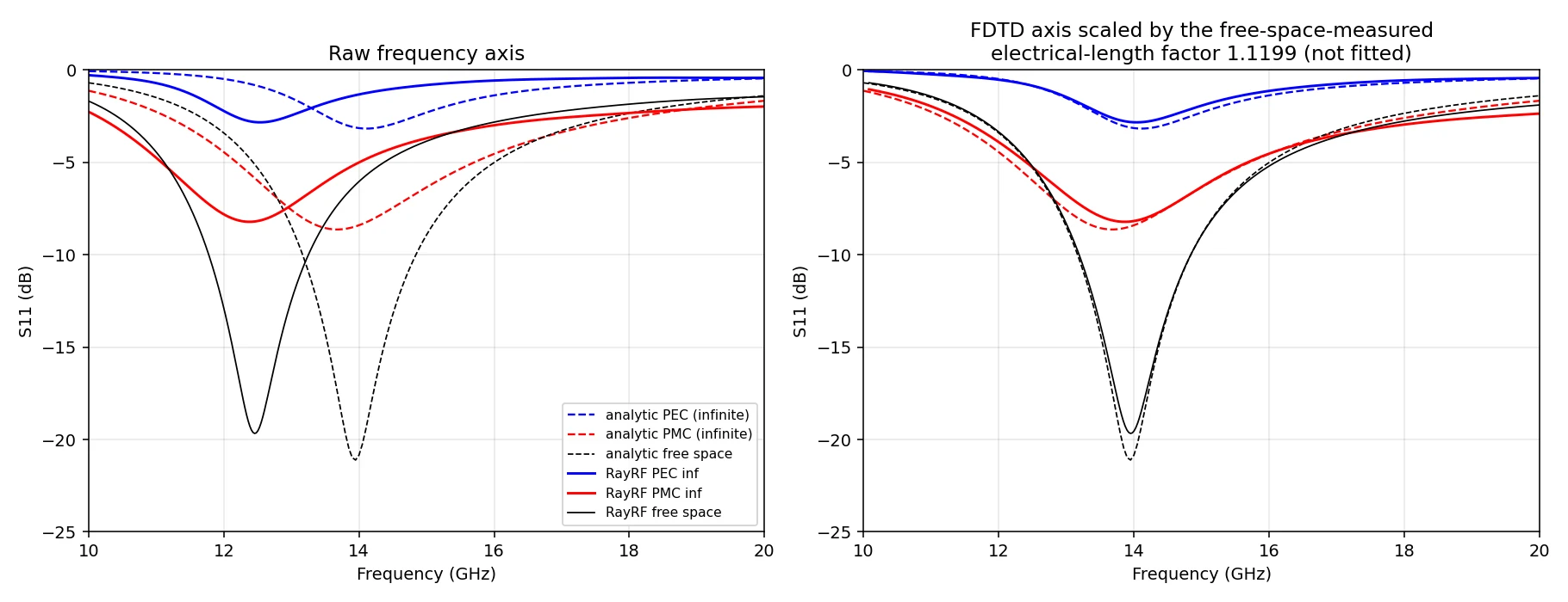
Those two identities are the core of the boundary validation. The feed model, the strip approximation and the staircased mesh all cancel in them, so what remains is whether the wall reflects with the right sign and the right magnitude. It does, for both polarities, and openEMS's PMC agrees through its own independent implementation.
The paper's main act: the mushroom EBG array
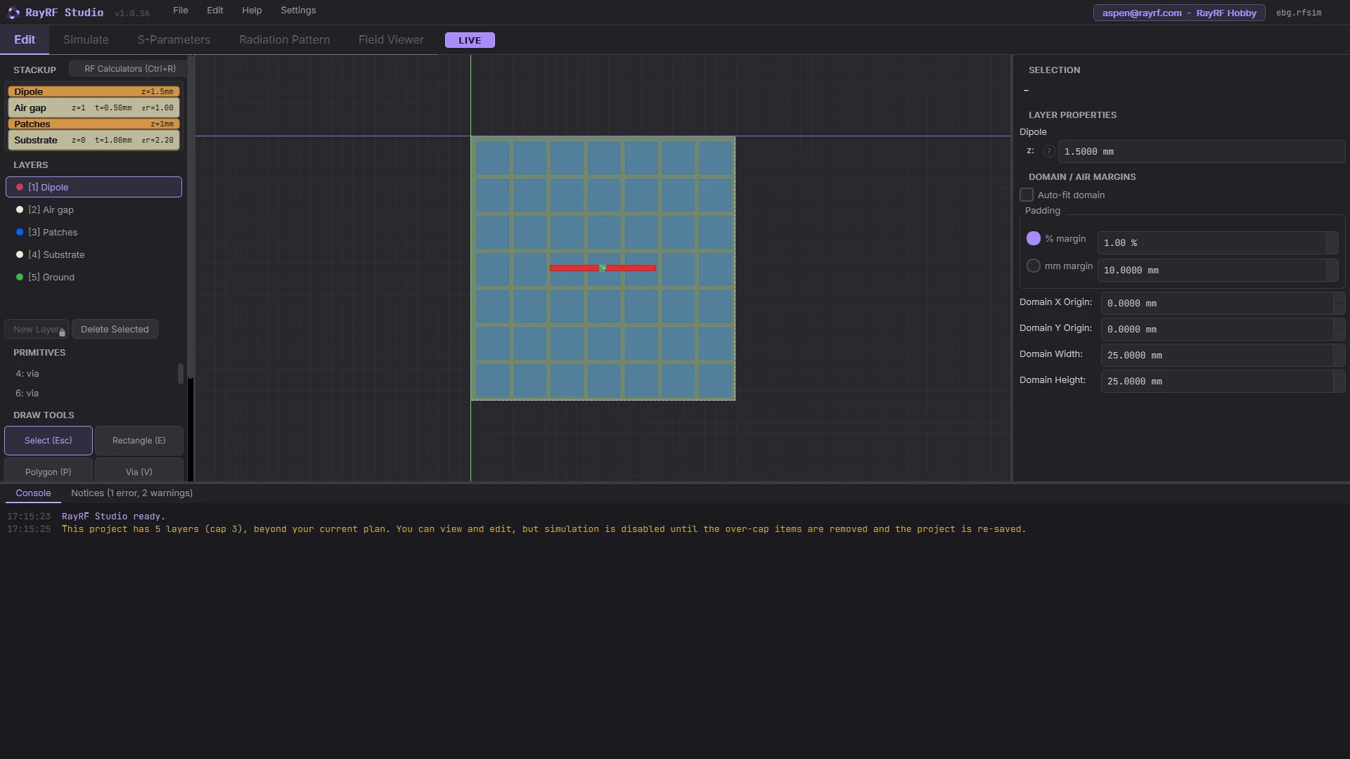
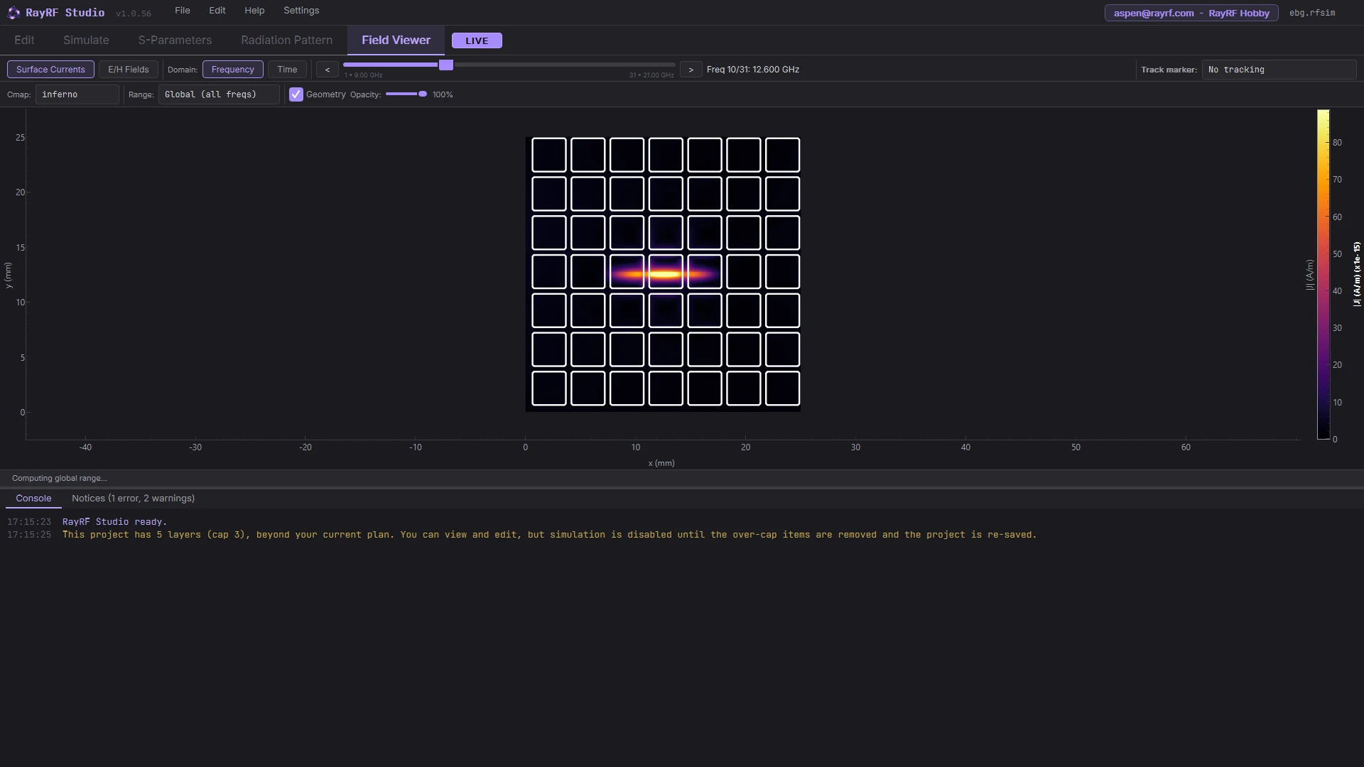
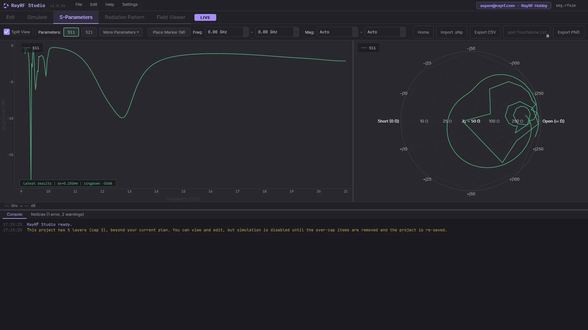
The reason this paper is famous is the third curve, so I built it. The EBG ground plane is a 7x7 array of 3.0 mm square patches with 0.5 mm gaps on a 1.0 mm substrate at eps 2.20, one grounding via per patch at 0.25 mm diameter, and the same dipole 0.5 mm above the patch tops. That is 49 patches, 49 vias, five stackup layers, and the same overall 1.5 mm antenna height as the PEC and PMC cases.
| Cell size | Cells | Steps run | Solver time | EBG dip | S11 |
|---|---|---|---|---|---|
| 0.5 mm | 0.66 M | 129,560 | 5.3 s | 11.98 GHz | -20.8 dB |
| 0.25 mm | 5.3 M | 163,640 | 46 s | 12.72 GHz | -10.0 dB |
| 0.125 mm | 42 M | 555,180 | 22 min | 13.73 GHz | -19.1 dB |
| openEMS, 0.25 mm | 5.3 M | 311,208 | 2 h 23 min | 12.67 GHz | -18.0 dB |
The EBG mechanism shows up at every mesh: a deep match dip in the right band with the input resistance pulled to 40 to 44 ohms, and the narrow low-band spikes of a lossless finite array sitting where the paper's curve shows its own ripple. At the matched 0.25 mm mesh, RayRF and openEMS agree on the dip position to 0.4 percent and both sit within about 1 percent of the paper. Depth at a deep match stays hypersensitive, which is why the three sources span -10 to -27 dB while agreeing on where the dip is. Across meshes the dip position still walks upward by 6 to 8 percent per halving, the strip artifact plus sub-cell features (0.25 mm vias, 0.5 mm gaps, the dipole 2 to 4 cells above the patches), so treat the absolute frequency as mesh-class dependent in any FDTD, this paper's own included. The starkest evidence for that: at the paper's 0.5 mm cell size, openEMS's geometric rasterizer closes the 1-cell gaps entirely and produces no EBG dip at all, while RayRF's mask-based rasterizer keeps the gaps and still resolves a clean -20.8 dB dip.
Replication found a real bug
This is what validation campaigns are for. The first EBG mesh ladder refused to converge in a way no setup variable could explain. I swept the board-to-boundary air spacing, the PML thickness, the excitation bandwidth and the step caps, and none of them moved the dip. What did explain it was in the solver: the via barrel zeroed the vertical E field through the cell at its end layer as well as the cells below it, which in RayRF's Yee convention extends the metal one cell past the top plate. Every mushroom via carried a spurious PEC stub poking into the air gap above its patch: all of the 0.5 mm gap at 0.5 mm cells, half at 0.25, a quarter at 0.125. Exactly the mesh-dependent loading the ladder showed.
The convention was provably inconsistent with the rest of the code: RayRF's own lumped port integrates the plate-to-plate voltage over the half-open cell range, which pins where a conductor sheet lives on the grid. The fix is the same half-open rule for the via barrel, applied to both the CUDA and CPU solvers. Geometries without vias are bit-identical before and after, the bundled patch example among them. With the fix, the coarse EBG rung moved 6.4 percent and the finer rungs barely moved, confirming the stub was the coarse-mesh distortion. A via stub one cell tall above a patch is irrelevant on a typical PCB. Under an antenna whose entire operating gap is two cells, it was not.
What does not line up, and why
The PMC here is a domain wall rather than a finite floating sheet, and a PMC cannot be measured against hardware because no such material exists. Published results, a second independent solver, and analytic theory together are the strongest available test for this feature, which is why this post exists.
Run it yourself
The archive has all seven projects, both solvers' outputs, and the analytic referee:
- projects/: the seven .rfsim files. The PEC-sheet, PMC and EBG cases ship with results embedded, so the S-Parameters, Radiation Pattern and Field Viewer tabs have data the moment they open.
- results/: RayRF S11 sweeps as CSV with columns freq_hz, s11_db, zin_real, zin_imag, plus the mesh ladder table.
- openems/: the driver script that reproduces the openEMS half of this post, and the four openEMS sweeps it produced.
- analytic/: image_theory.py and its output. Plain numpy, no RayRF required.
Download the validation kit (zip, 3 MB). Requires RayRF v1.0.55 or newer. The EBG project's five layers are above the Hobby plan's 3-layer cap, so re-running that one takes a trial or Pro license. Open a project, hit Run Simulation, and compare against the CSVs. If you find a discrepancy, I want to know about it.
For how RayRF holds up against physical hardware rather than a paper, the VNA validation page and the measurement write-up cover that side. The matched-mesh speed methodology is the same as the RayRF vs openEMS benchmark.
Per-face PML, PEC and PMC boundaries and in-plane ports are in RayRF v1.0.55. Draw the geometry, set the bottom face to PMC, and run. 30-day free trial, no card required.
Start the free trial